PlayStation 5 teardown: how Sony balanced build cost with performance
And why it's so large.

Last week, Sony finally unveiled its teardown of the PlayStation 5 console, fulfilling a promise first made by Mark Cerny over six months ago in his own Road to PS5 presentation. Effectively a basic outline of the make-up of the hardware, we finally got to see the fundamental building blocks of Sony's hulking console, but little was revealed in terms of the philosophy behind the remarkable design. Our take? It's a somewhat more conventional design than Xbox Series X, and the key challenges facing the designers are answered by sheer real estate.
Yahuhiro Ootori, VP of the mechanical design department at SIE is the stoic presenter of Sony's teardown - and he's the real deal, with a host of console patents to his name (the most recently unearthed being the PS5 dev kit) and of course, he also hosted the PS4 teardown video way back in 2013. His presentation begins with a basic outline of the port on the unit - a USB Type-A and 10Gbps Type-C on the front of the unit, paired with two 10Gbps Type-As on the rear, the LAN port and HDMI 2.1 output. We're hoping that confirmation of 10Gbps of bandwidth over USB should allow for some fast storage media options for back-compat titles, perhaps exceeding the results we've seen on Xbox Series X. Meanwhile, in revealing the rear ports, the sheer size of the venting here hints at the scale of the thermal solution to come.
Ootori seems to almost 'peel back' the white panels either side of the console before pulling them away. Under there, we get to see the dual inlets for the custom 120mm main fan. Of course, 120mm is a standard when it comes to building PCs but the 45mm depth of the custom unit is something else. It's also here where we see ducts designed for users to vacuum out excess dust that could clog up the cooling assembly. This was a major failing for PS4 and contributed to its increasing loudness of time and it's good to see this addressed without having to dismantle the unit and void the warranty - as was the case for the PlayStation 4 and PS4 Pro.
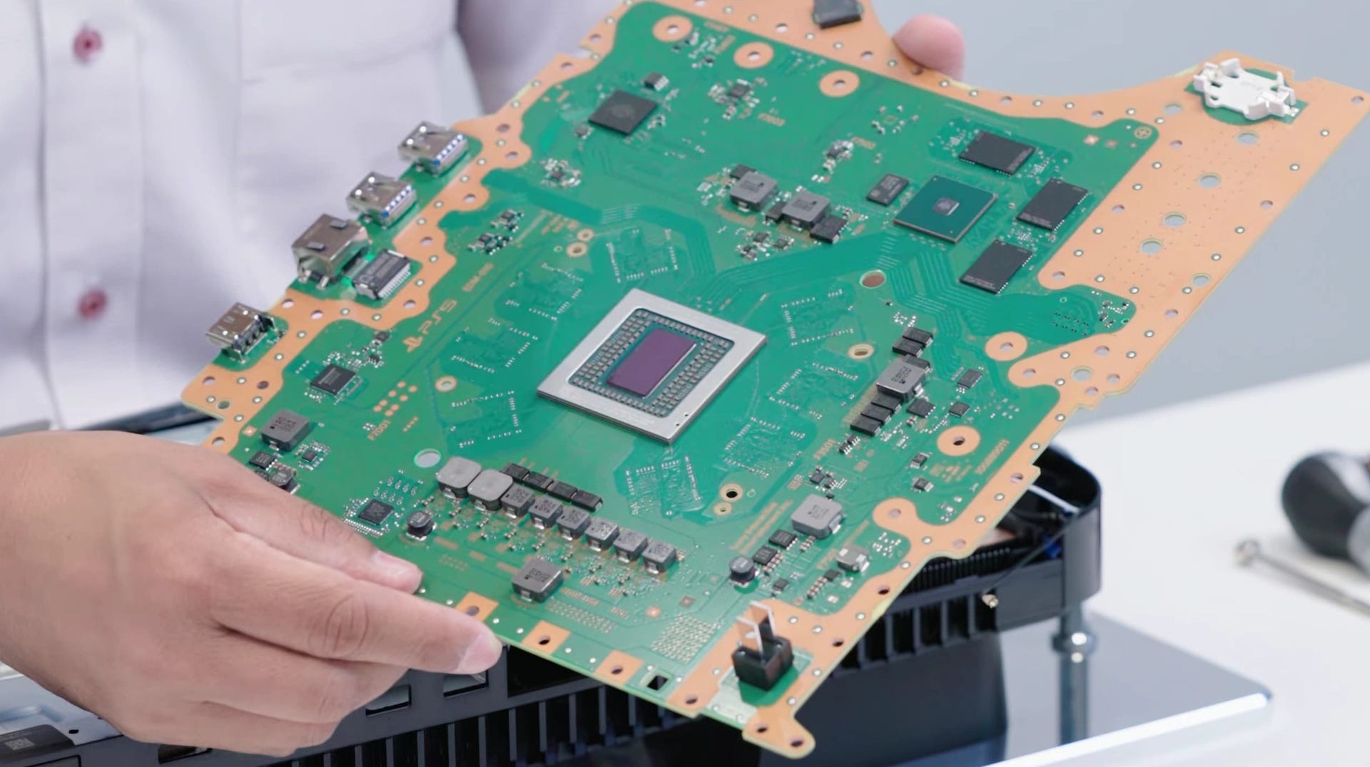
Once the WiFi and Bluetooth antennas are removed, shielding is taken away and we get our first look at the mainboard - a significantly simpler setup than the Microsoft Series X equivalent, which actually splits the whole design into individual processor and southbridge boards. There's only one board with PS5, the memory system is far less complex, and the board hardly looks packed by comparison. This is where we get our first look at the SoC (system on chip) - the main 'brains' of the system. Ootori himself describes this as a small, but highly clocked processor using a liquid metal thermal interface to ensure an optimal transfer of heat between the chip and the cooling assembly. This ticks off another noteworthy revision over PS4 and Pro, both of which were hardly renowned for the quality of their thermal grease.

The size of the SoC is interesting and often indicative of aspects of the design such as transistor count - not to mention having a big cost implication. Some online discussion suggests a 308mm2 chip, based on comparison to the GDDR6 layout seen around the main processor. With no square-on look at the chip, and no direct comparison points evident, getting a firm lock on the area of the processor is challenging, but something in the 305mm2 to 320mm2 seems likely when compared to Xbox Series X. Here, we have a fully annotated die shot and a confirmed area - stripping back 16 compute units and a couple of GDDR6 memory controllers certainly puts us in that ballpark. Compared to the Series X, the whole setup here in terms of the processor and the memory represents a significant cost saving.
The teardown also affords us a look at the SSD - built into the motherboard with the controller chip surrounded by NAND flash modules. The 5.5GB/s of raw bandwidth (even before factoring in the additional boost offered by hardware decompression) is a matter of record now - my only concern being that repairability and durability of SSDs are still something of a question mark. A defective console SSD basically makes repair impossible, beyond returning the unit to Sony. The M.2 storage expansion bay is also revealed - this is where the latest generation of PCIe 4.0 NVMe drives should have the requisite bandwidth to match Sony's internal solution, allowing off-the-shelf SSDs to be added for extra storage. The upgrade procedure looks simple enough, but these drives can get hot and I do wonder how the system aims to cool them - it's not clear from this video how this achieved.
The teardown ends with a look at the ginormous heatsink and a meaty 350W power supply (expect actual power draw to be a lot, lot lower). It's pretty clear what Sony's strategy is here with hardware design: to keep costs manageable with a small processor, but increase performance by blasting it with a high level of power, diverted to CPU and GPU frequencies as needed. Dissipating the heat is all down to what I'd consider an almost Toyota-like philosophy - not to reinvent the wheel (in the way that Microsoft has with Series X perhaps) but to rely upon what works and to add some extra flourishes where needed. The price we pay comes in terms of sheer volume: this is clearly going to be a huge console, relatively speaking, but the advantage to Sony is a considerable reduction in build cost.
Japanese influencers have been hands-on with the system and its silent nature has been commented upon - and I'll certainly be interested to see how that all stacks up once we're hands on with the hardware. Hopefully, that won't be too long now...