Switch's next Tegra X1 looks set to deliver more performance and longer battery life
Nvidia's cooking up a new chip - and details are starting to emerge.

This year's E3 delivered some impressive new Switch software, but hopes that Nintendo would reveal its hotly rumoured hardware revision - or hardware revisions - proved fruitless. The eagerly anticipated new Switches failed to materialise, but they should be appearing in the not-too-distant future - and while we know nothing about physical form-factors, the silicon at the heart of the new hardware is starting to come into focus. The standard Tegra X1 found within Switch is evolving and the evidence exists to demonstrate that both the mooted Switch mini and Switch Pro are possible targets offering improved performance, better battery life - or perhaps even both.
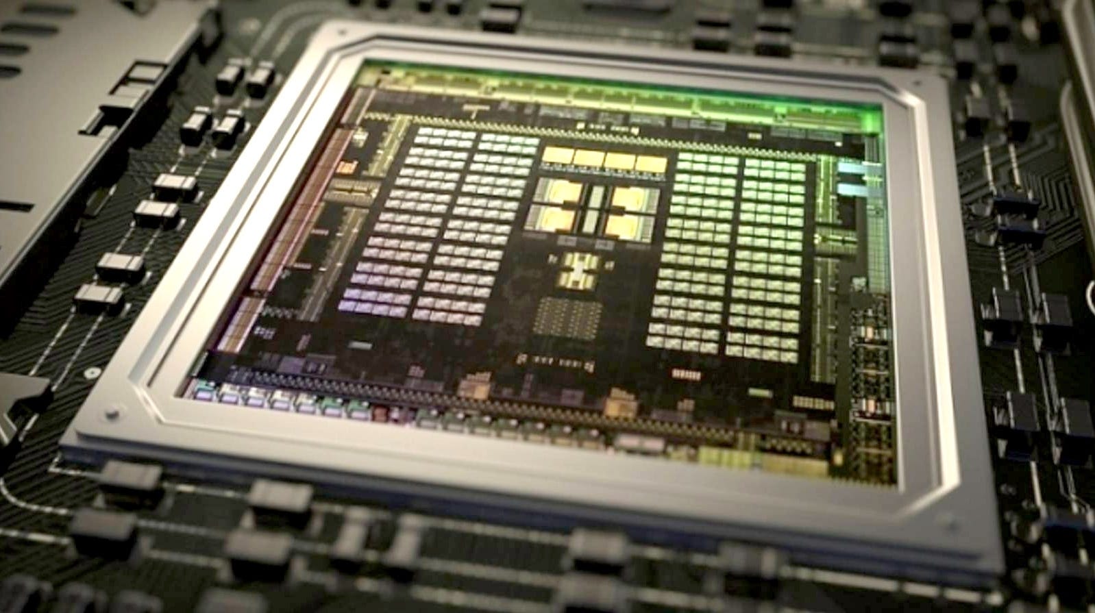
The Switch hardware upgrade story starts last year - specifically around March 2018 - when Nintendo released the 5.0 version of its system software, known internally as Horizon. Support for the standard 't210' version of the Tegra X1, codenamed Logan, was joined by a new, hitherto unknown revision: t214, also referenced as Mariko. Nvidia's Tegra codenames are based on the real names of superheroes (Parker being Tegra X2) but Mariko is something different. Back in the day, she was a love interest for Logan/Wolverine in the Marvel comics - the obvious inference being that this is a partner chip, not a new product. Beyond that, little else was revealed - though Mariko seemed to be matched with 8GB of memory, a potential 2x upgrade for a retail Switch - or an extra 2GB for dev kits (we had a look at one during E3 - it reported 6GB of RAM in dev mode, 4GB in retail mode).
But what t214/Mariko actually is and how it differs from the standard Tegra was not immediately obvious - but it did seem to go beyond patching the security leaks that have made the Switch such fun for hackers to tool with. In recent weeks though, the story has moved on. The OG Switch debuted around the same time as a hardware revision for Nvidia's Tegra X1, found within the 2017 revision of the Shield Android TV micro-console/streamer - and featured nigh-on identical silicon to the Switch. Evidence suggests that the same thing is happening again - the Google Play Developer Console Device Catalogue is listing a new Shield, based on a t210b01 chip. So what's the connection between this and the t214 Mariko?
For answers, we looked to ResetEra's Thraktor, whose short post managed to link the dots between the two chips, with the evidence all but confirming that both processors are actually one and the same. The Era post is brief, but Thraktor himself gave us the references needed to piece more of the story together - and it's all out there in public, for anyone to see if they dig deep enough. Outside of Switch, Tegra hardware is more typically used in open source environments such as Linux and Android, meaning any one can take a look at the source and adapt it.
Github commits like this one and this one both replace t214 with t210b01 with the commit message, "Should use t210b01 in any code/comment". There are other smoking guns linking the two processors too - here, here and here, for example - where commit messages refer to t214 while the code or filenames reference t210b01 instead. Another piece of evidence Thraktor points out to us is that Nvidia uses the MAX77812 voltage regulator for the new t210b01, and the exact same component is used for t214 within the Switch firmware.
At this point, it seems almost certain that whatever new processor is found within the upcoming Shield Android TV revision has been supported in Nintendo's firmware for around 15 months now, but what we don't know is what the chip actually is. We can rule out a component that would have been a great fit for a new Switch - Tegra X2. This has much faster clocks, doubles up on memory bandwidth and features a very similar GPU to the X1, while retaining the ARM A57 cores found in the t210. Tegra X2 has found a home in automotive systems and the Magic Leap augmented reality glasses, but its t186 designation rules it out of contention as Mariko. Whatever powers the revised Nintendo console(s) and the Shield is something different.

And it's at this point where firm knowledge starts to give way to what are perhaps outdated specifications and a good amount of theory crafting. Producing another t210 - albeit a b01 version - suggests a good old-fashioned hardware revision, a new version of the existing silicon. The chances are that switching away from Tegra X1's old 20nm fabrication process towards a more current manufacturing method would save a lot of money and allow Nintendo to refresh the range. Smaller chips allow for higher frequencies up to a point, plus they run on lower voltages. In short, a refresh at this point allows the Switch to potentially produce more performance, less heat, extending battery life while being cheaper to manufacture.
And there is evidence to suggest that this is indeed the case. DVFS tables for the t210b01 are available, and they can be compared to the standard t210. Operating voltages are indeed reduced, and while CPU and GPU frequencies supported by t210 are retained, faster clocks are also available. The GPU limit of the Tegra X1 - specced at 1GHz but with a max 921MHz on Switch - is increased to 1.267GHz on the new processor. It's worth noting that the frequency data for the new processor is rather old and may reference an incomplete engineering sample chip, and things may be different in the final production chip - but at the very least we have an idea of what Nvidia is shooting for with this silicon.
Of course, short of exploiting an older Switch and using an overclocking tool like SysClk, users will never have access to the maximum Tegra X1 clocks for their consoles - though Nintendo itself is now 'overclocking' the console itself in various fascinating ways. Limiting clocks improves battery life and reduces heat, putting less strain on the active cooling assembly within the hybrid console. Regardless, the option is there for Nintendo to use the presumed process advantages not just for improved efficiency and battery life, but performance too.

With regards t210b01's improvements, higher clocks and lower voltages suggest a drop from a 20nm processor design down to 16nm FinFET instead - but Tegra X1 was always an outlier, a production chip running on an experimental fabrication process Nvidia never chose to pursue for its mainstream GPUs - and I wonder if the firm is following the same procedure with its replacement, mitigating the cost of exploring 7nm technology by sharing costs with Nintendo. Only a teardown of the new Switch revision(s) will give us the physical dimensions that allow us to firmly identify how the t210b01/t214 is manufactured, but the increase in clocks seen in the DVFS tables would likely favour 16nmFF, a mature process and a good fit for a mass-produced console.
And it's important to note is that the evidence does suggest that t210b01 is fully compatible with the original Tegra X1 - the DVFS table for the new chip lists all of the clock speed modes available, not just the maximums, and the modes used in existing Switch games are all in the line-up - it's just that this list is longer, with more frequencies supported at the higher end. And with that in mind, standard Switch performance could likely be achieved with no cooling assembly required at all, meaning that a prospective Switch mini wouldn't just be smaller with more battery life, it could be silent too. Meanwhile, a decent performance uplift on the GPU side could obviously improve frame-rates and image quality in a range of games using dynamic resolution scaling. Based on the clocks in Nvidia's documents (though again, this may be outdated info) there wouldn't be a revelatory increase in system performance - nothing like a generational leap as such, or even anything as profound as the jump from 3DS to New 3DS, but it would still be a valuable addition.
While I would expect Nintendo to tie down new performance modes from a potential Switch Pro to new games or patches for existing titles, the advent of SysClk for exploited consoles has proven that just about any game can work with overclocking, even if the net improvements vary on a title by title basis. In short, while we shouldn't get our hopes up too much, a PS4 Pro-style boost mode could theoretically be incorporated, with extra resources enabled for all legacy titles. While possible and with precedent on other consoles, it does seem unlikely that Nintendo would allow users to overclock their consoles - but we can hope!
The stage is set then - something is happening, new Tegra X1 silicon is almost certainly en route and we now have some idea of its capabilities. And as a bonus, a potentially chunky GPU bump for the Shield Android TV would certainly help in improving a bunch of games available on that system too - and while Switch is the focus for much of the anticipation, we could see a new form factor and a cheaper price for Nvidia's impressive little streamer too.