Wii U graphics power finally revealed
Hard facts on the Nintendo GPU emerge. So is it more powerful than PS3 and Xbox 360?
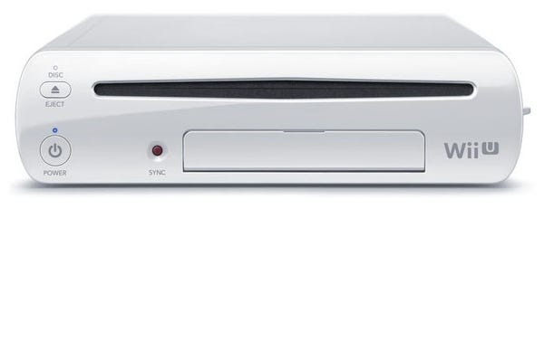

Despite its general release two months ago, Nintendo's Wii U console would remain something of a technological mystery. We quickly gained a good idea of the make-up of the IBM tri-core CPU, but the system's apparent strengths are in its graphics hardware, and in that regard we had little or no idea of the composition of the Radeon core. Indeed, it's safe to say that we knew much more about the graphics processors in the next-generation Xbox and PlayStation. Until now.
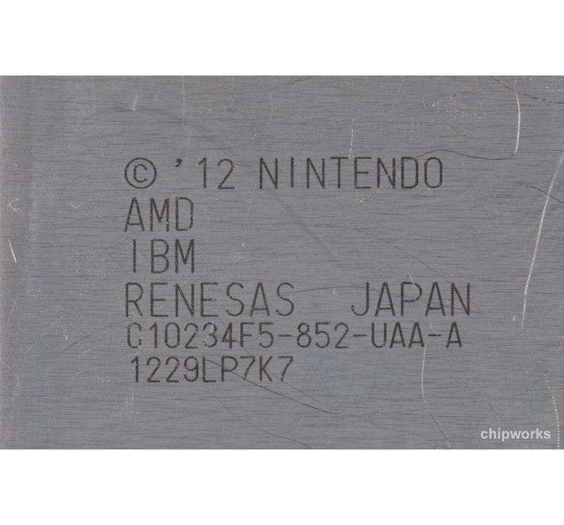
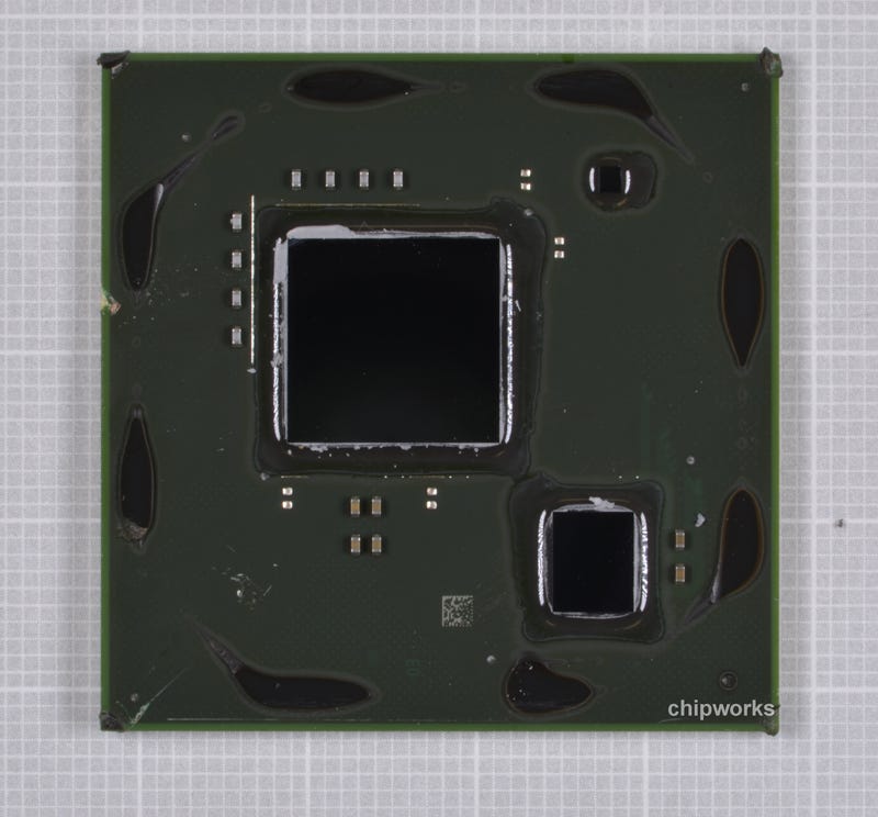
Detailed polysilicon die photography of the Wii U's GPU has now been released, showing the hardware make-up at the nano level and resolving most of the outstanding mysteries. However, the story of how these photos came into existence is a fascinating tale in itself: community forum NeoGAF noticed that Chipworks were selling Wii U reverse-engineering photography on its website, with shots of the principal silicon being offered at $200 a pop. Seeking to draw a line under the controversy surrounding the Nintendo hardware, a collection was started to buy the photos.
There was just one problem. The shots were simply higher quality versions of what had already been revealed on sites like Anandtech - good for getting an idea of the amount of silicon used and the make-up of the overall design, but without the ultra-magnification required to provide answers, and therefore no further use in unearthing the secrets of the Wii U hardware. At this point, Chipworks itself became aware of the community money-raising effort, and decided to help out by providing the required shot - for free. It's a remarkably generous gesture bearing in mind that the cost of carrying out this work is, as Chipworks' Rob Williamson told us, "non-trivial".
"Sourcing the images required to nail down the make-up of the Wii U GPU was the result of a remarkable community effort, plus the generosity of reverse engineering specialists, Chipworks."
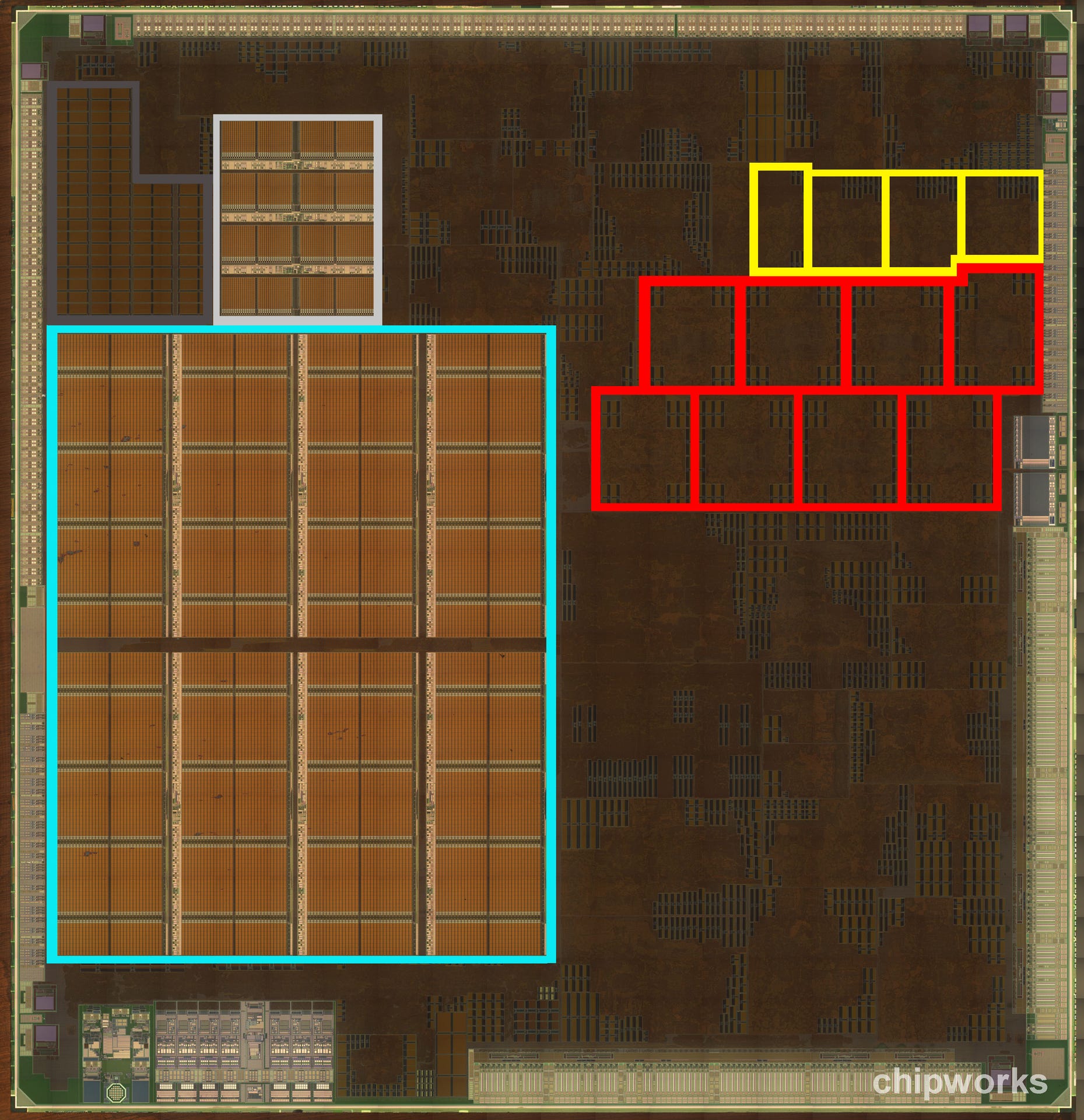
So, what does the new shot below actually tell us? Well, first of all, let's be clear about how we draw our conclusions. Graphics cores work principally by spreading work in parallel over a vast array of processors. On the die shot, this manifests as the same mini-blocks of transistors "copied and pasted" next to one another. We know that the Wii U hardware is based on AMD's RV770 line of processors - essentially the Radeon HD 4xxx cards - so we have some point of comparison with existing photography of equivalent AMD hardware.
Chipworks' shot is still being analysed, but the core fundamentals are now seemingly beyond doubt. The Wii U GPU core features 320 stream processors married up with 16 texture mapping units and featuring 8 ROPs. After the Wii U's initial reveal at E3 2011, our take on the hardware was more reserved than most. "We reckon it probably has more in common with the Radeon HD 4650/4670 as opposed to anything more exotic," we said at the time. "The 320 stream processors on those chips would have more than enough power to support 360 and PS3 level visuals, especially in a closed-box system."
It was ballpark speculation at the time based on what we had eyeballed at the event, but the final GPU is indeed a close match to the 4650/4670, albeit with a deficit in the number of texture-mapping units and a lower clock speed - 550MHz. AMD's RV770 hardware is well documented so with these numbers we can now, categorically, finally rule out any next-gen pretensions for the Wii U - the GCN hardware in Durango and Orbis is in a completely different league. However, the 16 TMUs at 550MHz and texture cache improvements found in RV770 do elevate the capabilities of this hardware beyond the Xenos GPU in the Xbox 360 - 1.5 times the raw shader power sounds about right. [Update: It's generally accepted that the PS3 graphics core is less capable than Xenos, so Wii U's GPU would be even more capable.] 1080p resolution is around 2.5x that of 720p, so bearing in mind the inclusion of just eight ROPs, it's highly unlikely that we'll be seeing any complex 3D titles running at 1080p.
All of which may lead some to wonder quite why many of the Wii U ports disappoint - especially Black Ops 2, which appears to have been derived from the Xbox 360 version, running more slowly even at the same 880x720 sub-hd resolution. The answer comes from a mixture of known and unknown variables.
"Plenty of questions remain about the Wii U hardware, but this die-shot tells us everything we need to know about the core make-up of the Radeon graphics processor."
The obvious suspect would be the Wii U's 1.2GHz CPU, a tri-core piece of hardware re-architected from the Wii's Broadway chip, in turn a tweaked, overclocked version of the GameCube's Gekko processor. In many of our Wii U Face-Offs we've seen substantial performance dips on CPU-specific tasks. However, there still plenty of unknowns to factor in too - specifically the bandwidth levels from the main RAM and the exact nature of the GPU's interface to its 32MB of onboard eDRAM. While the general capabilities of the Wii U hardware are now beyond doubt, discussion will continue about how the principal processing elements and the memory are interfaced together, and Nintendo's platform-exclusive titles should give us some indication of what this core is capable of when developers are targeting it directly.
However, while we now have our most important answers, the die-shot also throws up a few more mysteries too - specifically, what is the nature of the second and third banks of RAM up on the top-left, and bearing in mind how little of the chip is taken up by the ALUs and TMUs, what else is taking up the rest of the space? Here we can only speculate, but away from other essential GPU elements such as the ROPs and the command processor, we'd put good money on the Wii U equivalent to the Wii's ARM 'Starlet' security core being a part of this hardware, along with an audio DSP. We wouldn't be surprised at all if there's a hardware video encoder in there too for compressing the framebuffer for transmission to the GamePad LCD display. The additional banks of memory could well be there for Wii compatibility, and could account for the 1MB texture and 2MB framebuffer. Indeed, the entire Wii GPU could be on there, to ensure full backwards compatibility.
While there's still room for plenty of debate about the Wii U hardware, the core fundamentals are now in place and effectively we have something approaching a full spec. It took an extraordinary effort to get this far and you may be wondering quite why it took a reverse engineering specialist using ultra-magnification photography to get this information, when we already know the equivalent data for Durango and Orbis. The answer is fairly straightforward - leaks tend to derive from development kit and SDK documentation and, as we understand it, this crucial information simply wasn't available in Nintendo's papers, with developers essentially left to their own devices to figure out the performance level of the hardware.