Inside Nvidia's new hardware for Switch 2: what is the T239 processor?
A new, custom Tegra heavy on machine learning and ray tracing.

Way back in June 2021, noted technology leaker kopite7kimi posted a detailed picture of Nvidia's T234 processor, revealing for the first time that Nintendo would be receiving a customised variant, dubbed T239. In the two years that followed, a wealth of overwhelming evidence has essentially confirmed that they were right. The T239 is an advanced mobile processor, based on an octo-core ARM A78C CPU cluster, paired with a custom graphics unit based on Nvidia's RTX 30-series Ampere architecture, combined with some backported elements from the latest Ada Lovelace GPUs - and with an all-new file decompression engine for fast engine. It also supports Nvidia's console-specific graphics API, all but confirming that it's destined for the next generation Switch.
In this piece, we'll talk about the various evidence that links the T239 with Nintendo and we'll also be taking a look at the closest equivalent mobile GPU in the graphics space, downclocking it to ultra-low frequencies in an attempt to get some kind of handle on what a low-power Ampere-based graphics core can offer, whether ray tracing is possible and just how important DLSS upscaling could be for a second generation Nintendo hybrid handheld/console. We'll also see whether our analysis marries up with any of the sparse information gleaned from the Gamescom showing of Switch 2 to select developers.
But let's kick off with a basic, fundamental question. Can we say for sure, with absolute 100 percent certainty that the T239 is indeed the Switch 2 chip? That's a negative. However, we can definitely tie the T239 to a Nintendo project and there's no evidence - and indeed, no need - for Nvidia to create this chip for anyone else. For its own endeavours in the automotive and robotics market, the firm already has the T234. And to understand the custom variant, it's a really good idea to get to know what the T234 is and why Nintendo couldn't use this chip to begin with.
After all, going back to the first Switch, no custom processor was involved at all. Despite marketing from Nvidia to suggest otherwise when the Nintendo hybrid was announced, the chip at the centre of the machine was vanilla Tegra X1, albeit with some elements (such as its lower core CPU cores) disabled. Designed from the get-go for the tablet, phone and gaming market, Tegra X1 was a dud until Nintendo co-opted it for Switch, where it found a new lease of life. For Switch 2, Nvidia has nothing in the parts bin that's appropriate for a successor. The latest Tegra processors - like the T234 - are built for an entirely different, more demanding market. The building blocks are there for a great mobile chip, but the existing configuration is just too large and bloated for a streamlined, mainstream console.
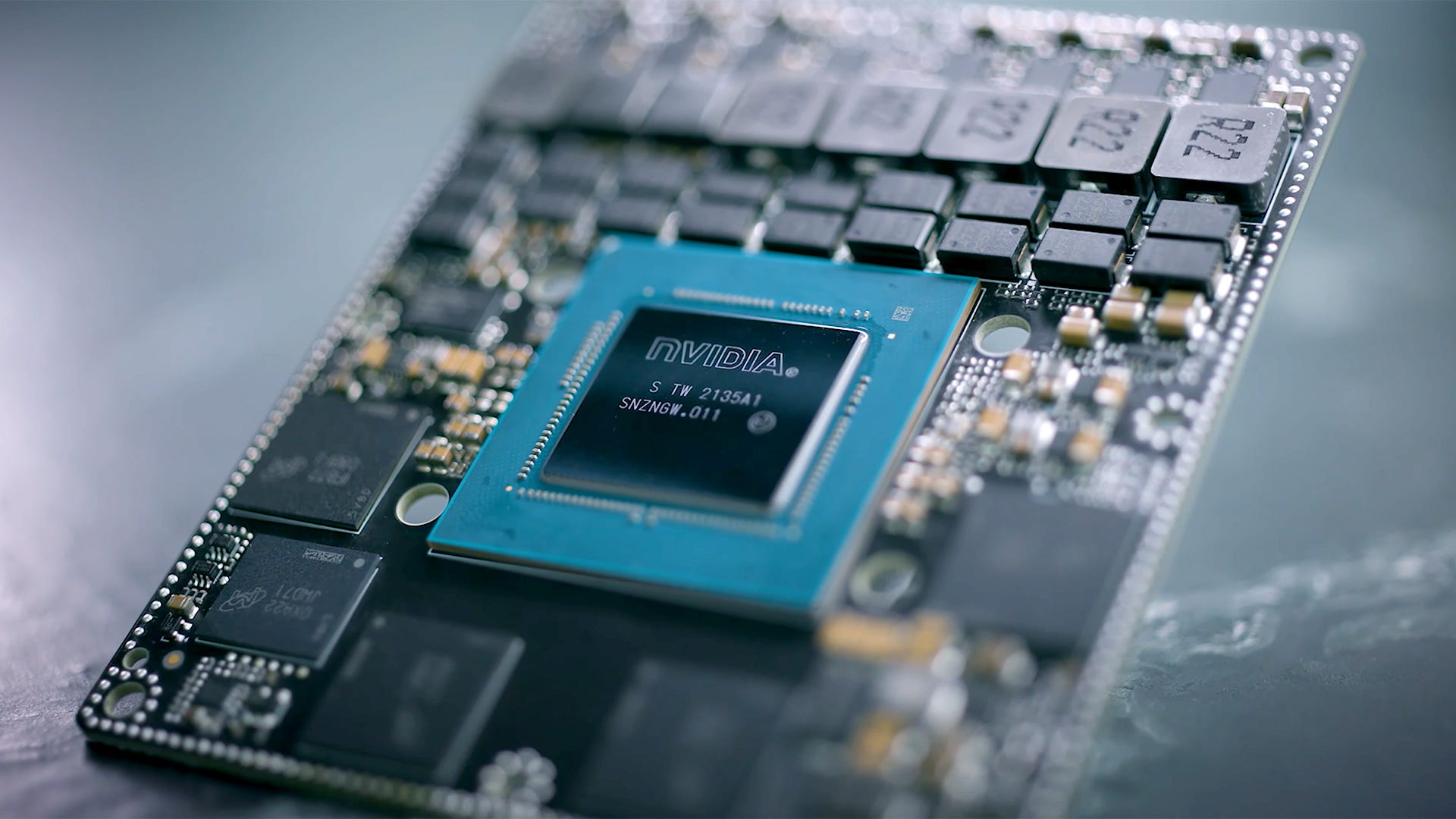
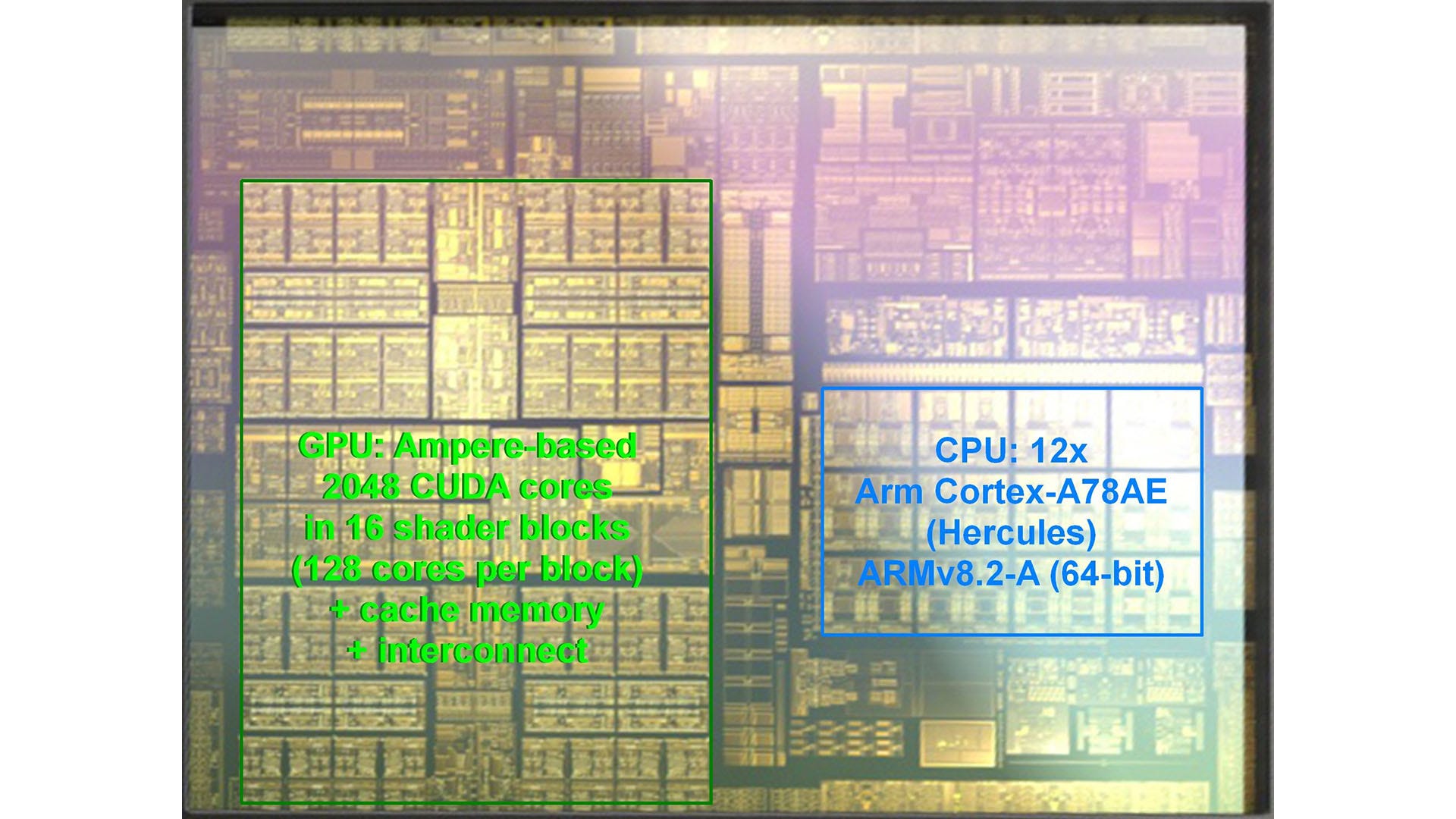
Let's be clear here: the existing T234 is a monster of a chip. With a die size of 455mm2, it dwarves the Xbox Series X processor at 360mm2. It's fabricated using the same Samsung 8nm technology used for the RTX 30-series cards, so it's actually a step behind the 7nm and 6nm processes used in current-gen consoles. CPU-size, it features 12 ARM A78AE CPU cores, paired with a GPU based on the 30-series Ampere architecture with 2048 CUDA cores and a 256-bit memory interface. For the automotive and robotics market, T234 requires a lot of machine learning performance, so there's also a deep learning accelerator built in - and its capabilities can be augmented by the tensor cores within the GPU.
Nvidia's T239 - its next-generation gaming processor
What's immediately clear is that the T234 is simply too big to work in a mobile product. At 455mm2, this processor is much larger than the 392mm2 RTX 3070, and with a mixture of common sense reasoning, leaks, a big Nvidia Hack and inappropriate LinkedIn posts from Nvidia and ex-Nvidia staff, we have a good picture of what form T239 will take. Also crucial is that Nvidia maintains its own Linux distribution and while much of it is private, there are enough references to T239 in there to get a handle on the make-up of the processor.
The CPU cluster will be quite different than T234's, for starters. While the A78 ARM cores are commonplace, the AE variant is built to meet stringent standards set by the Automotive Electronics Council, with half the cores used to verify the work of the other half - totally inappropriate for a games machine. Nvidia's Linux distribution suggests that T239 has eight CPU cores in a single cluster, strongly suggesting ARM's A78C will be used.
| Nvidia T234 | Projected T239 | Nvidia RTX 2050 4GB | |
|---|---|---|---|
| CPU Architecture | 12x ARM A78AE | 8x ARM A78C | - |
| GPU Architecture | Ampere | Ampere | Ampere |
| CUDA Cores | 2048 | 1536 | 2048 |
| Memory/Interface | 256-bit/LPDDR5 | 128-bit/LPDDR5 | 64-bit/GDDR6 |
| Memory Bandwidth | 204GB/s | Max 102GB/s | 96GB/s |
Memory bandwidth is crucial for a mobile gaming machine and it's the primary performance bottleneck in the current Switch. The 256-bit interface in T239 is wildly extravagant for a mobile games machine, and Nvidia's Linux update suggests a 128-bit interface, almost certainly paired with LPDDR5 memory. We should expect absolute maximum bandwidth of 102GB/s, but of course, Nintendo can choose to downclock that for improved efficiency. Support for DisplayPort - easily configurable for HDMI - is in T239, as it is in the standard Switch. The difference here is that there's enough bandwidth for full HDMI 2.1 support, assuming Nintendo uses it.
Other spec leaks derived from Nvidia's Linux distribution are intriguing. There's a full media encode/decode block on T239 and although the chip uses RTX 30-series Ampere architecture, the media block is backported from the latest Ada Lovelace chips, so it should be faster with support for more formats, including AV1. Improved clock-gating - a way of improving efficiency from dormant silicon - is another Ada feature that has somehow found its way into T239. Power consumption is a bit of a hot potato when it comes to discussing this chip, for a variety of reasons I'll tackle shortly.
Nvidia's Linux distro also confirms that T239 has an optical flow accelerator - a core component of DLSS 3 frame generation. The problem here is that it's the last generation Ampere rendition, not the Ada Lovelace rendition that Nvidia deemed good enough to make frame-gen happen. Whether it has a role to play in a potential Switch successor remains to be seen, but it's interesting that the block was retained when Nvidia architected this custom, cut-down Tegra.
There's one more component of T239 worthy of comment - the FDE. It's an entirely new hardware block not found in the T234. FDE stands for File Decompression Engine. Similar to the decompression block found in PlayStation 5, this basically allows for ultra-fast decompression of assets from storage and into memory. There was a recent report from Nate The Hate talking about a Breath of the Wild demo running on Switch 2 hardware with zero loading times. Well, T239 has the hardware to facilitate ultra-fast loading, but it's going to need a much faster storage format to make that possible - an area where we are lacking details right now.
The Linux details paint a very detailed picture of the T239 and many of these details were confirmed by an Nvidia hack - the Ampere GPU architecture, the 128-bit memory bus and LPDDR5 memory, along with the backported power saving features from the Ada Lovelace design. The hack also suggests that T239 has 1536 CUDA cores, 75 percent of the cores of the much larger T234.
We now have a chip that's a significantly cutdown Tegra, with redundant features removed and a file decompression block added. There are a few question marks though. What clock speeds should we expect from CPU and GPU? How fast will the memory run? This is a question that's key to understanding performance limitations in a mobile processor. There's also the question of whether T239 has the deep learning accelerator from the T234 or not. I believe this is crucial to a potential Switch 2 and its use of DLSS upscaling.
On the clocks question, Nvidia provides a tool for calculating power consumption on the T234 and it suggests that the GPU is most efficient at 540MHz, a good candidate for handheld clocks. Efficiency drops alarmingly the faster you clock it, and the more power required, the more heat is generated. I'd be surprised if docked clocks exceeded 1GHz and it could be a fair degree lower. 1.0GHz also looks like the sweet spot for CPU clocks too. However, these are calculations for a larger Tegra chip that's definitely on the 8nm Samsung process. A smaller chip could be more efficient and right now, there's no evidence that confirms absolutely that it is still on the inefficient Samsung 8nm process (though I suspect it is).
What kind of performance should we expect from T239?
So, to summarise so far, we've got a detailed idea of the specs for a chip dubbed T239 that's been in development for several years, which was first leaked over two years ago and has since been referenced several times in Nvidia's Linux distribution and was mentioned in the Nvidia hack and in several posts from Nvidia staff on LinkedIn. But there's more: a smoking gun, if you will. When the original Switch was developed, Nvidia created a low-level graphics API for getting the most out of the CPU and GPU hardware. It was called NVM. The Nvidia hack describes an NVN2 graphics API. It suggests that several pieces of Nvidia hardware can be used with NVN2 but there are several sections of code where it's explicit that it's emulating T239 behaviour on that other hardware. In short, Nvidia has refactored an existing Tegra to be smaller, more efficient and equipped with fast loading hardware - and it's using a next-gen rendition of the Switch's NVN graphics API.
So, what should expect from the T239 in a mobile games machine? In the recent Microsoft FTC court case, Activision's Bobby Kotick mentioned that Nintendo had briefed him on the device last year and its performance profile was in line with last-gen hardware. Well, that may well be the case but one could equally say that the Switch had similar horsepower to the Wii U or Xbox 360 but it punched well above that weight. This was achieved via a more modern GPU and more memory, for starters. I'd venture to suggest that Switch 2 follows that trend - and goes further. I mean, Bobby Kotick talks about PS4-class performance, but meanwhile we're hearing talk of The Matrix Awakens on Unreal Engine 5 running on it, something a PS4 could never do. This is what happens when you have custom silicon based on a much more modern GPU, equipped with machine learning tensor cores and hardware accelerated ray tracing.
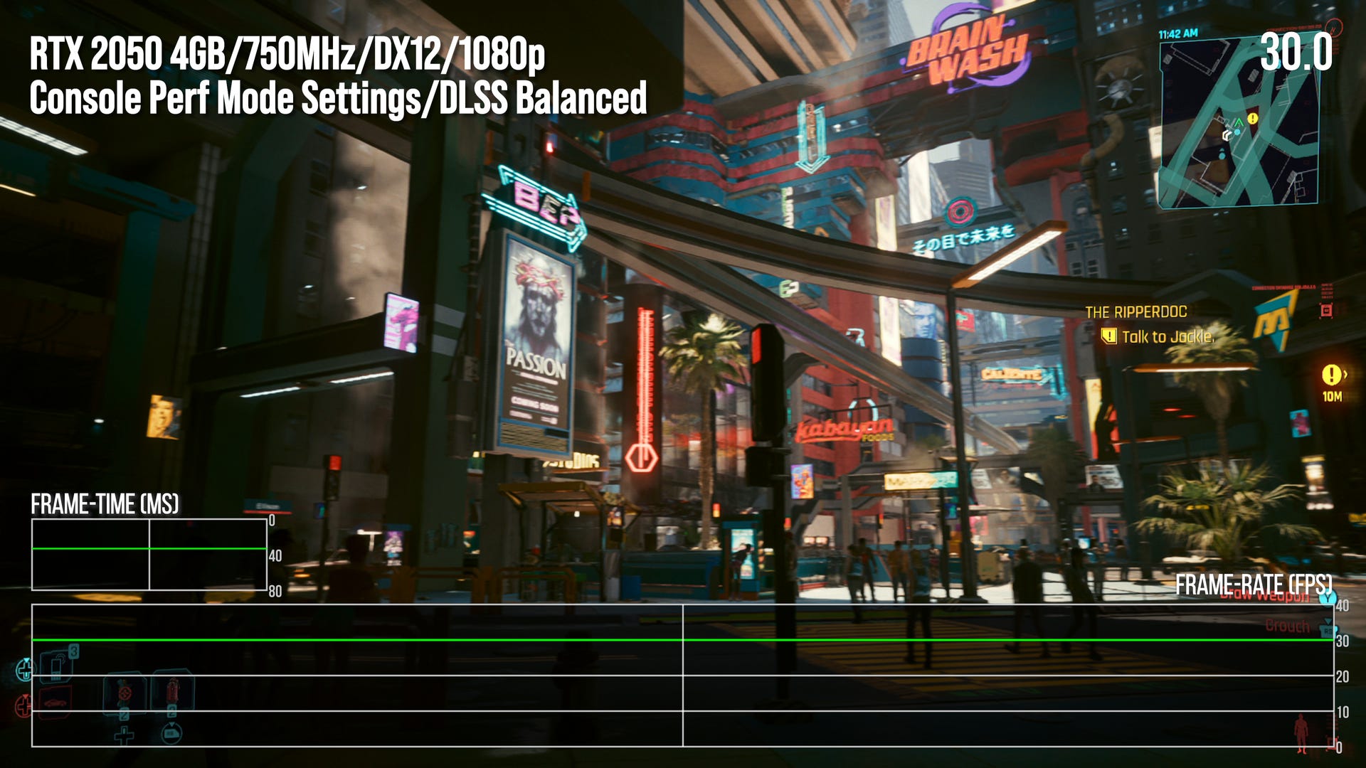
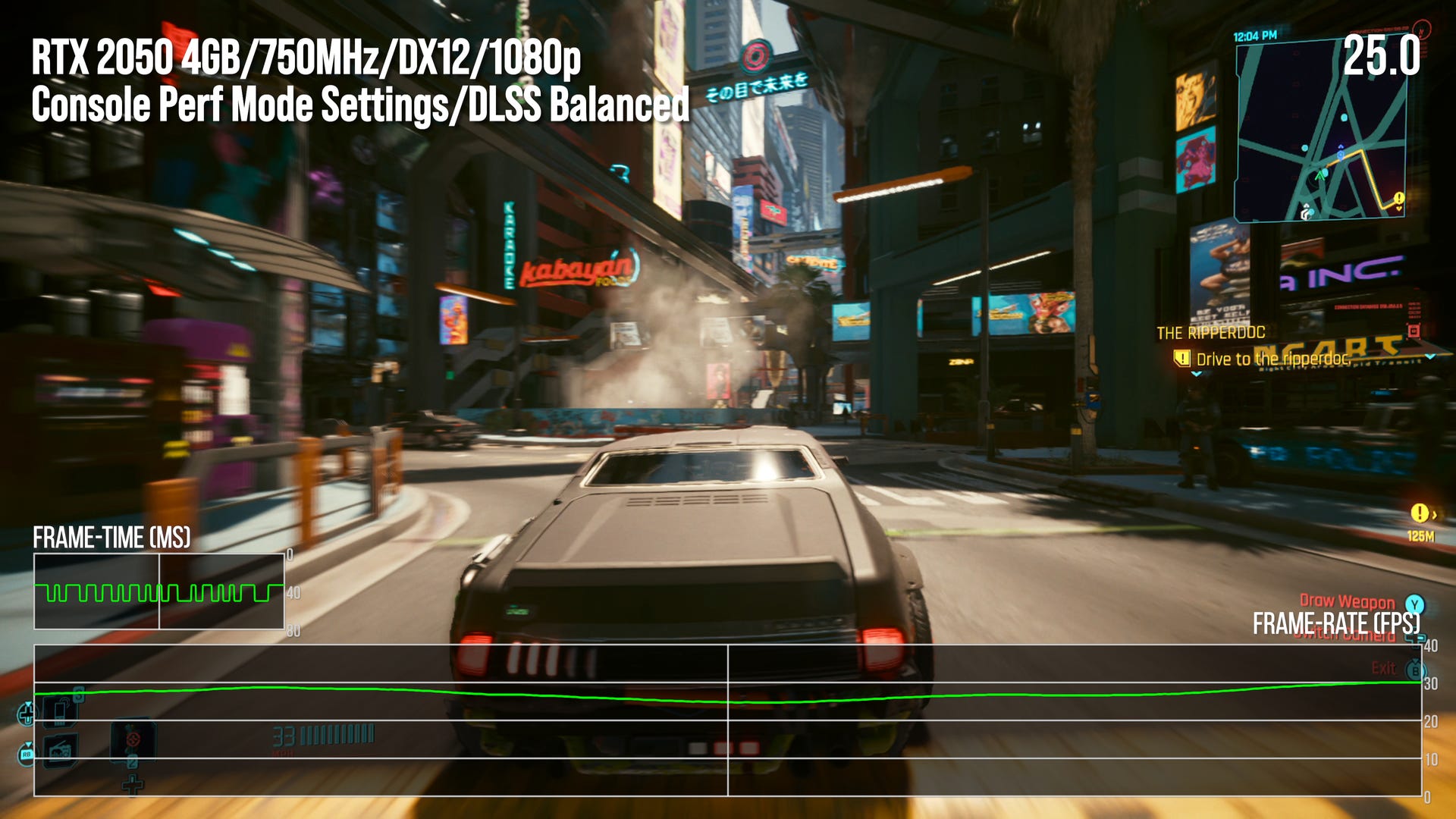
To get some idea of what a mobile Ampere-class processor can do, I turned my hand to some practical work. There's no real equivalent counterpart for the capabilities of the A78C CPU cluster in the PC space, but when it comes to the GPU, we can get close. I bought in a Dell Vostro 5630 comes equipped with the following specs: a Core i7 1360p CPU, 16 gigs of 4800MHz LPDDR5, a 512GB SSD and an RTX 2050. It's that last component we're looking at more closely here.
First of all, despite its designation as an RTX 20-series part, it's actually the exact same silicon as the Ampere based RTX 3050 and 3050 Ti - it's a GA107 processor. We can't match the 1536 CUDA cores of the T239, but 2048 CUDA cores is the lowest we can go on a gaming Ampere GPU. So why not simply get a 3050 laptop then? Well, think of the 2050 as a lobotomised 3050 - it has a lower power budget, lower clocks and crucially, it's got a 64-bit memory interface. At 96GB/s of bandwidth, it operates with a considerable bottleneck compared to the RTX 3050 but it also gives us ballpark equivalence with the bandwidth a potential Switch 2 could deliver. There's one sticking point though - the 2050 only comes with 4GB of RAM. I'd expect to see 8GB or even 12GB of total system memory in Switch 2.
You'll see the results of my tests in the video atop this page, but before we go on, let's be clear: this is the closest approximation we can get together for the T239 GPU, but more accurately, what you're seeing in the video is an ultra low-spec Ampere GPU running at meagre clock speeds, starved of memory bandwidth. It can only really give us a ballpark idea of what a mobile Ampere chip can deliver, even when I downclocked it to a ridiculously low 750MHz - but even so, the results are intriguing.
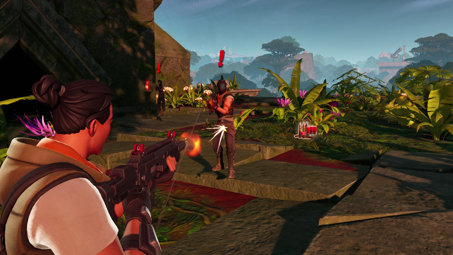
I couldn't get The Matrix Awakens running owing to the 4GB memory limitation on the RTX 2050 and it seems that the demo requires around 5.6GB at the minimum. However, the fully enabled Fortnite UE5 experience using Lumen, Nanite and Virtual Shadow Maps does work. Indeed, unlike the console versions, we do actually have access to hardware accelerated ray tracing in the PC version and yes, it does run on the RTX 2050 laptop. I tested hardware RT Lumen, its software variant, and I also tested at native 720p and several DLSS variants, all resolving to a 1080p output. For the record, software RT with DLSS performance mode (540p in, 1080p out) is the winner but between best and worst results here, there's just a 9.5 percent difference, and in fps terms that's just 2.82fps.
My guess is that the Matrix Awakens demo for Switch 2 based on target hardware probably is real, but Epic must be doing a lot of work in making Unreal Engine 5's key features run well on the new Nintendo machine, simply because The Matrix Awakens is a lot heavier on the GPU than Fortnite. That being the case, just running PC code on a low power Ampere GPU isn't likely to be that revealing. Still, it does run. You can use hardware RT. DLSS is helpful.
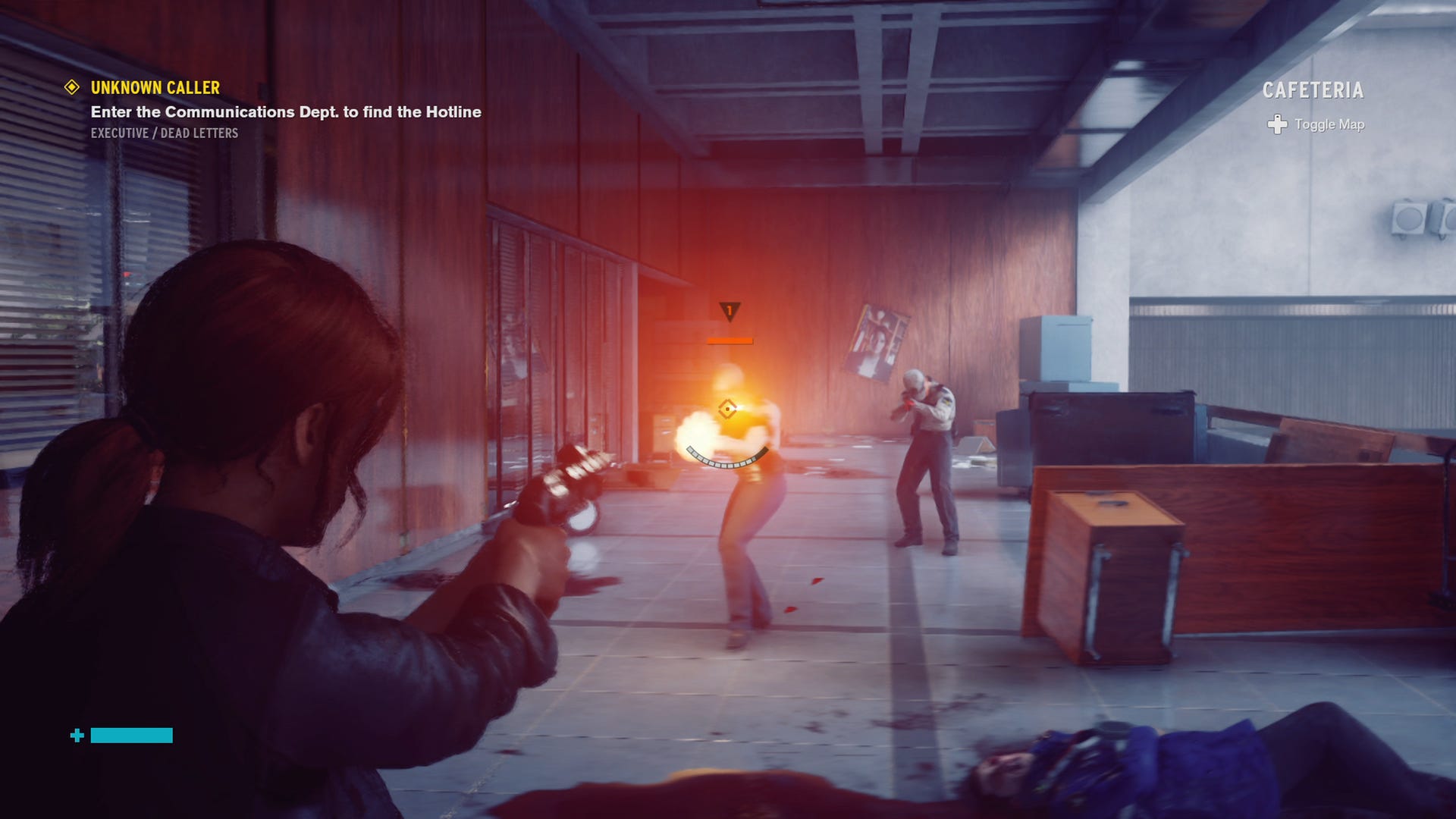


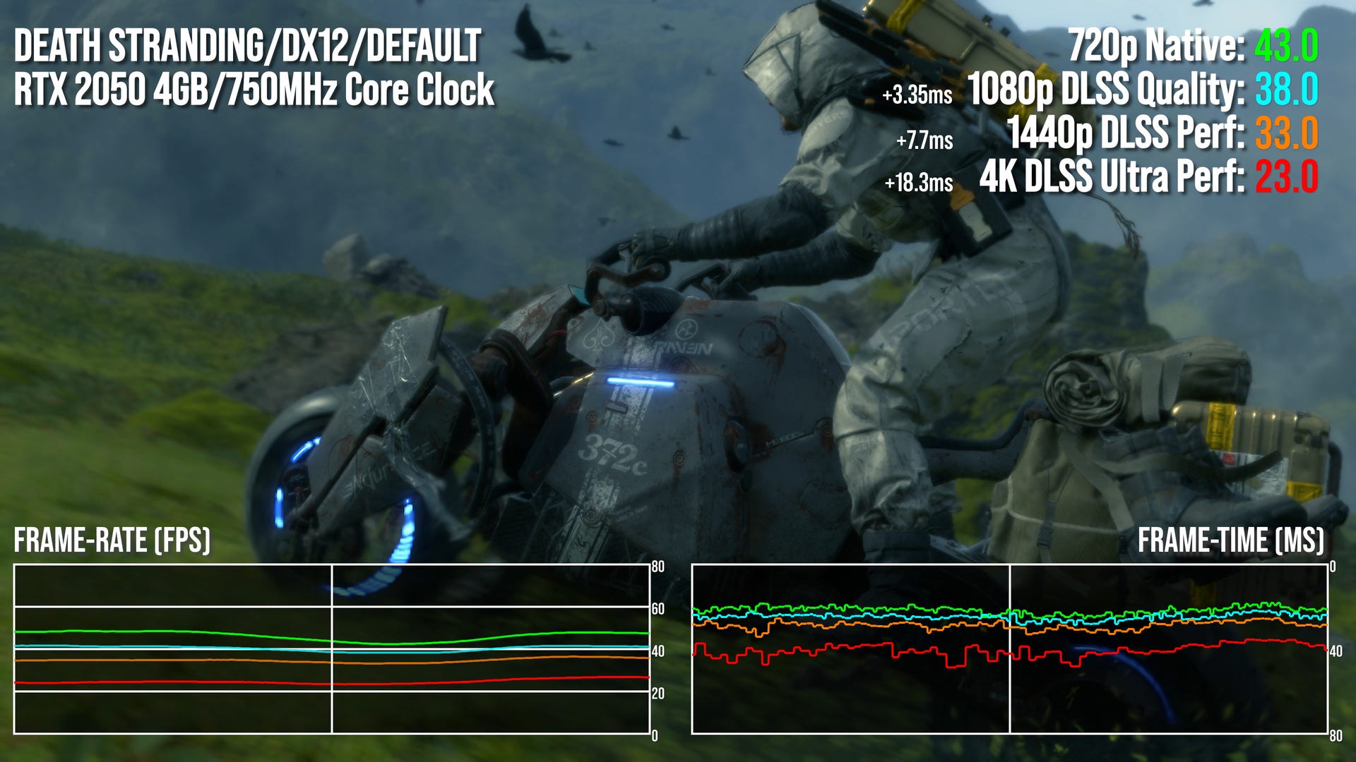
I also tried Death Stranding, benchmarking its GPU-heavy intro. At 1080p native, the sequence averages at 34.9fps, which does support the last-gen horsepower narrative. At 720p, frame-rate rises to 52.5fps. I've also run this bench at DLSS quality mode too - 67 percent of native res. 34.9fps average increases to 44.7fps. At 720p with DLSS, frame-rate does increase but the performance differential is difficult to accurately measure because the sequence is actually capped at 60fps. Still, looking at gameplay, 1440p in DLSS performance mode is viable on this little Ampere-based GPU and while much of the game played out locked at 30 frames per second, there were some dips beneath. In a confrontation with the BTs, the heavy post-processing seemed to be too much for the GPU to cope with.
DLSS support: useful for Switch 2 or absolutely crucial?
I believe that DLSS is crucial to the next Nintendo machine, but whether we'll get the fabled 'Switch 4K' comes down to whether a core component of the original T234 has made its way into T239. I'm referring to the Deep Learning Accelerator - a separate hardware block that can combine its own processing with the tensor cores within the GPU. My tests with the RTX 2050 suggest that DLSS could be useful for upscaling to 1080p and perhaps even 1440p, as we saw in Death Stranding. However, the higher the output resolution, the higher the cost of DLSS. In Death Stranding, the additional cost of upscaling 720p to 4K (DLSS ultra performance mode) is over 18ms. For a 60fps demo, just the processing cost of DLSS exceeds the 16.7ms render time for the complete frame. However, if the DLA has made its way from T234 to T239, DLSS will have far less of a computational cost.
It's also important to stress how important DLSS is to the whole Switch 2 enterprise. As you'll see in the video, all of our gameplay tests produced some relatively impressive results - but all required the use of DLSS, upscaling from various internal resolutions to 1080p. So, in the PC space, it's generally considered that it's 'OK' to run the upscaler at performance mode at 4K, balanced mode at 1440p and quality mode at 1080p. Console gaming in the living room is different, you're sat much further away from the screen and image quality expectations are different. After all, we've seen some remarkably low resolution already this generation, even from PS5 and Series X.
So, I actually think for a mobile chipset attached to a living room display, 1080p performance mode upscaling from a native 540p will look acceptable, while 1080p from native 720p (DLSS quality mode) looks pretty great. It'll certainly look a lot better than most of the demanding Switch games we've seen in docked play. DLSS 4K ultra performance mode upscaling from a native 720p? Again, check it out in the video above - it's far from a pristine 4K, but a low-power console doesn't need to mimic native 4K. It just needs to provide a decent image on a 4K living room TV.
And that's basically where I'm up to right now with Switch 2, its technological make-up and the kind of ballpark performance that an ultra-pared back Ampere GPU can deliver. There is still controversy and many unresolved questions. There are some who believe that the T239 was intended for a scrapped 'Switch 4K' or 'Switch Pro' and that the actual next generation Switch will offer something different. I don't agree with this: the level of investment required to make T239 and the size of the GPU along with its custom blocks represents a proper, next generation leap over the Tegra X1.
Questions and concerns: is T239 viable for a handheld?
However, there are some more legitimate questions and concerns over the T239. We've established that the 455mm2 T234 is way, way too large for a mobile games processor - but even with its various cutbacks in CPU and graphics, the T239 will likely be much larger than the 118mm2 Tegra X1 in the current Switch. A larger chip requires meatier cooling which may not be a good match for a Nintendo hybrid handheld/home console. Some believe that T239 isn't on the 8nm Samsung process node at all, and it's likely that only a teardown of the retail machine will confirm this one way or another.
From my perspective, the bottom line is that by a process of elimination, T239 is the best candidate for the processor at the heart of the new Nintendo machine. Nvidia's Jensen Huang is on the record as saying that Nvidia's partnership with Nintendo will likely last two decades. And with a mooted 2024 release date, there have been no convincing leaks whatsoever for any other processor that could find its way into the new Switch.
I had fun putting together those practical tests with the RTX 2050 and it gives you some idea of what the lowliest Ampere-based GPU can offer. Any modern game seems to run just fine on it, assuming you adjust settings accordingly. And DLSS is - once again - a game-changer and potentially even more transformative if the Deep Learning Accelerator block is in there.
But just let me stress one more time that this is only the closest approximation we can make to the mooted T239 spec: while clocks are low, CUDA cores are higher. While memory bandwidth is paltry in PC terms, it's ballpark with the best that T239 could offer - and Nintendo may choose to downclock. And of course, in our tests, there's no contention on that bandwidth from the CPU - another potential drain on performance.
Even so, there's promise here - and remember that I am using PC versions of the games I tested, with no scope for customisation for a mobile platform. And really, the magic is going to come from the developers themselves. Take a look back at when Doom 2016 first appeared on Switch, or The Witcher 3, or the Crysis remasters, or the amazing ports produced by Rebellion North like the Sniper Elite and Zombie Army games. These games defied the technological limits of the Tegra X1 and regardless of the T239's specs, I expect to see the same next time around too.
Switch 2: the big questions we have no answers for
Some of our outstanding questions around the next generation Switch will likely get some answers once we see the hardware. How big is it? What kind of battery life is being promised? What will the games look like? To what extent can existing Switch hardware - including its JoyCons - work with its successor? We may also get some further disclosure from Nvidia itself on the role it has played in the development of the machine.
Based on everything I've learned about T239 over the months, I think my biggest surprise is how ambitious the hardware is. Given the chance to re-architect a new, games-centric processor, Nvidia could have followed the route it laid down with its GTX 16-series graphics cards by stripping out machine learning and RT hardware, or paring them back to the minimum with cut-price alternatives (like the way AMD integrated hardware RT into RDNA 2 with an emphasis on the lowest silicon cost possible). Instead, the evidence suggests that Nvidia and Nintendo have agreed on a design that arguably over-delivers on next-gen features, while the File Decompression Engine (FDE) points to quality of life additions to the silicon that a firmly orientated around a great gaming experience. Could this be the most forward-looking hardware design from Nintendo since the GameCube?
And while questions remain around using Samsung 8nm silicon, there is a silver lining for Nintendoin delivering a revised model further down the line. It could embrace 6nm, 5nm or 4nm technologies for improved thermals and battery life, just as it did with the revised Switch, the OLED model and Switch Lite. In the short term, the question is how large T239 will be and if its characteristics mean we need a larger handheld - something I don't think Nintendo would want.
Right now, the various leaks and unofficial disclosures mean that we likely know far more about the internals of the next Nintendo machine than we do about other more important elements - like the whole concept of the new hardware, for example. T239 is a mobile-orientated processor, while Nintendo's centralisation of all development resources to one platform means that we're almost certainly looking at another Switch, as opposed to some kind of brand new concept. However, with Nintendo's history, a straight Switch 2 seems almost too simple - but with initial disclosure hopefully not too far away, hopefully we'll have a better perspective on the new machine soon.