What's inside the Wii U?
Nintendo conducts its own pre-release teardown of the new hardware, revealing plenty of surprises.

Who needs an iFixit Wii U teardown? In a remarkable turn of events, the latest Ask Iwata interview sees the Wii U tech team reveal the innards of its own console - and there are some fascinating aspects to the design of the new hardware.
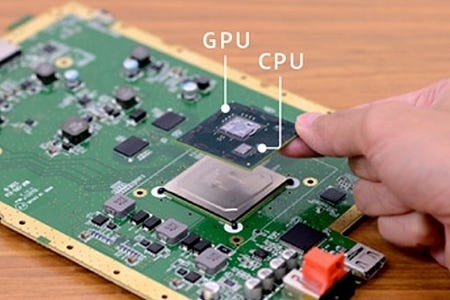
Some elements of the discussion between Iwata and his engineering team essentially confirm what we already know - that the Wii U offers up the first Nintendo-designed multi-core console, but the team pointedly skirt around the number of cores featured (it is almost certainly three). However, much of the interview concerns the revelation that Nintendo has employed a MCM - a multi-chip module - to house the crucial CPU and GPU combination. It's not a single chip design along the lines of the Xbox 360S, but it's a hugely important component of the Wii U's design.
"This time we fully embraced the idea of using an MCM for our gaming console," says Genyo Takeda, senior managing director and general manager of the Integrated Research and Development Division.
"An MCM is where the aforementioned multi-core CPU chip and the GPU chip are built into a single component. The GPU itself also contains quite a large on-chip memory. Due to this MCM, the package costs less and we could speed up data exchange among two LSIs while lowering power consumption. And also the international division of labour in general, would be cost-effective."
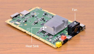
IBM supplies the CPU for Wii U, while Nintendo has partnered with AMD for the graphics core. Building those into a single package proved to be rather challenging, especially when faults arose during the design process, but adopting the MCM strategy centralises heat on the mainboard. This makes it easier to dissipate heat with a less expensive cooling assembly, and helps immensely in making the Wii U a significantly smaller unit overall than the PS3 Slim or the Xbox 360S.
"The major takeaways from this surprise reveal are the efficiency of the overall design and the respective sizes of the Wii U's CPU and graphics core."

"Lowering power consumption has been our position since the GameCube. By putting LSI chips in this small package, the power necessary for communication between LSI chips drastically fell," says Ko Shiota, Takeda's deputy in the R&D division.
"And by putting them in a single small package, we can make the footprint on the CPU board smaller. For the contribution it would make to casing miniaturisation too, I wanted to do it no matter what!"
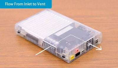
Despite the integration of CPU and GPU onto a single module (the original Wii uses discrete components, each cooled individually), the Nintendo engineering team reveal that the new console outputs three times as much heat as its predecessor, meaning the Wii U's chassis design was massively important in keeping the machine cool. Fan placement was refined over time and even the design of the external grates was adapted to improve air-flow.
The team also spend a lot of time dwelling on the durability of the console, presumably to put consumers' minds at rest after the RROD and YLOD debacles from times gone by. Our concern with Wii U has always been about the concentration of so much heat within so small a casing - the MCM design mitigates this to a certain degree by centralising components, but 3x Wii heat output is still a significant thermal challenge. Nintendo ran what it describes as "ageing tests", where components are stressed over a long period to ensure they stand the test of time.
"If you don't do that, defects will eventually arise when the product is in the customers' hands. Toward the end of creating the product, a lot of tests that take a long time are left over, so it took an extra long time to analyse each single defect," says Nobuyiki Akagi of Nintendo's product development department.
The team also discuss the hardware back-compat with the original Wii - an important feature for Nintendo bearing in mind the colossal install base for the best-selling console of this generation.
"The designers were already incredibly familiar with the Wii, so without getting hung up on the two machines' completely different structures, they came up with ideas we would never have thought of," Shiota says.
"There were times when you would usually just incorporate both the Wii U and Wii circuits, like 1+1. But instead of just adding like that, they adjusted the new parts added to Wii U so they could be used for Wii as well."
"The Wii U is a tiny unit and even with the innovative MCM solution we do worry about the ability of the modest heatsink and fan to cope with three times the heat of the original Wii."
And here's where we stray into somewhat controversial territory, as it appears that the tri-core IBM CPU has less in common with the POWER7 "Watson" architecture we were promised, with plausible rumours suggesting a multi-core evolution of the same CPU found in the original Wii - and by extension, the 2001 vintage GameCube. If there's one thing that's rather striking about Nintendo's Wii U teardown it's the minuscule die area occupied by the CPU in relation to the relatively massive GPU from AMD.
In time, exact die sizes will be calculated by comparing the parts to standard-sized components elsewhere on the mainboard (the HDMI port, for example) but first impressions reinforce the current position that Wii U's design is skewed towards a more feature-rich graphics core with rather more modest CPU power. There will be comparisons with Microsoft's Xbox 360 integrated CPU/GPU which shows more balance in terms of die area between the two major components, but it's worth pointing out that Nintendo appears to have integrated its 32MB of eDRAM into the graphics core itself, while it remains a daughter die on the 360. Other functions - such as I/O - may also be integrated in order to centralise heat as much as possible.
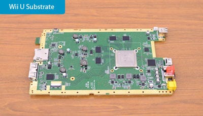
And if there's one thing that stands out as even more surprising than the MCM implementation, it's the spartan nature of the mainboard: very basic indeed even compared to the revised PS3 CECH-400 super-slim motherboard. While there may still be some surprises on the reverse side of the mainboard, what we see on the face is very simply designed - and thus less expensive to build. Nintendo talks about power efficiency constantly in this Ask Iwata piece, but that goes hand in hand with overall production economics. It looks like an elegant design - something very, very different from the current generation consoles from Sony and Microsoft - and somewhat minimalistic too.
In the mainboard pictures Nintendo provides, we see the MCM module with metallic heatspreader surrounded by what looks like four memory modules (best guess is that these are DDR3 in nature, 512MB a piece), and the only other major chip appears to be at the rear of the board, next to the HDMI socket - so presumably a video output controller. We're quite curious as to where the wireless transmission technology is housed - the board itself looks rather sparsely populated to the point where you wonder if it couldn't be miniaturised still further.
In all, this is a fascinating sneak-peek at the contents of the new Wii U console, offering up plenty of surprises - without even factoring in any kind of look at the GamePad controller with its "without latency" video transmission link. Iwata says that's coming up in the next article...