AMD reveals HBM: the future of graphics RAM technology
As GDDR5 hits insurmountable limits, AMD's new stacked memory is smaller, faster and more power-efficient.


AMD has officially unveiled its next-generation graphics memory solution - HBM: high bandwidth memory. Sporting an enormous increase in throughput over existing GDDR5 technology, along with equally impressive power-efficiency plus impressive space-saving attributes, HBM is set for release on AMD's next flagship graphics cards, with the firm confirming that we should see these on sale within two months. Radeon R9 390X, any one?
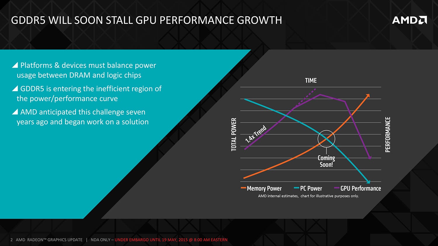
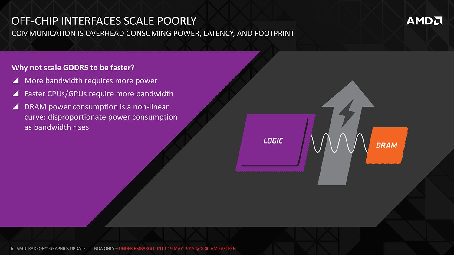
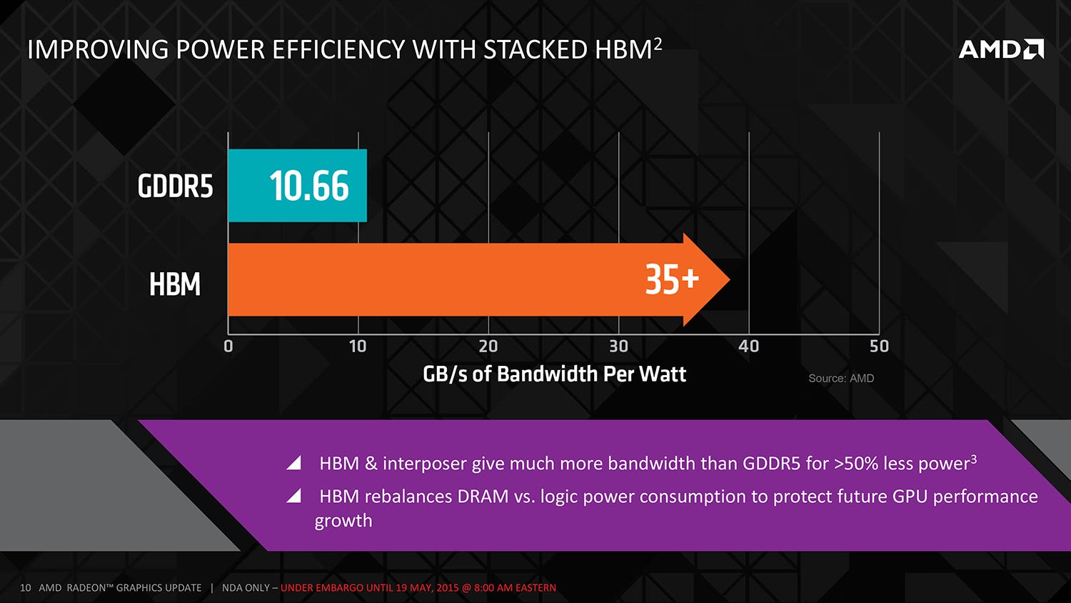
We attended a conference call presentation last week, given by Joe Macri, CTO of computing and graphics at AMD. He talked about the reasons behind the development of HBM - specifically that while GPUs were becoming increasingly more powerful, the existing GDDR5 memory system wasn't scaling in line. He explained that 7gbps chips are available now, with 8gbps modules in the pipeline, but there's little future in the tech: the amount of power needed to increase memory bandwidth doesn't scale in a linear fashion - the faster GDDR5 becomes, the more power hungry it is. GPUs tend to have hard TDP (thermal design power) limits, and going forward, it doesn't make sense to funnel large amounts of power through to the memory system, when more is achieved by diverting it to the GPU core.
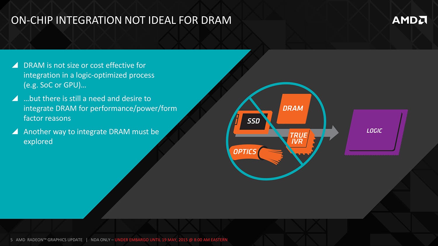
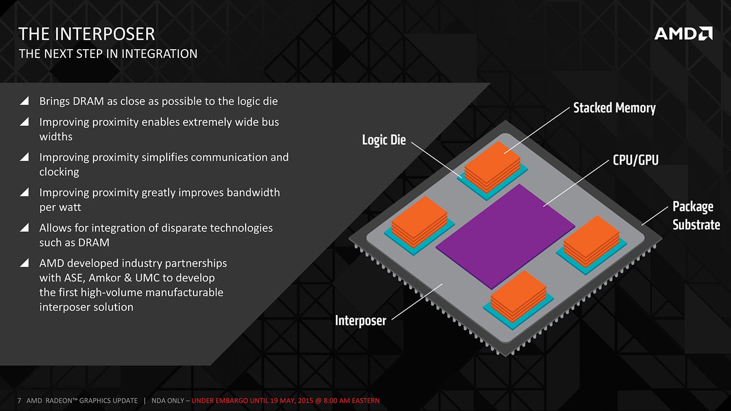
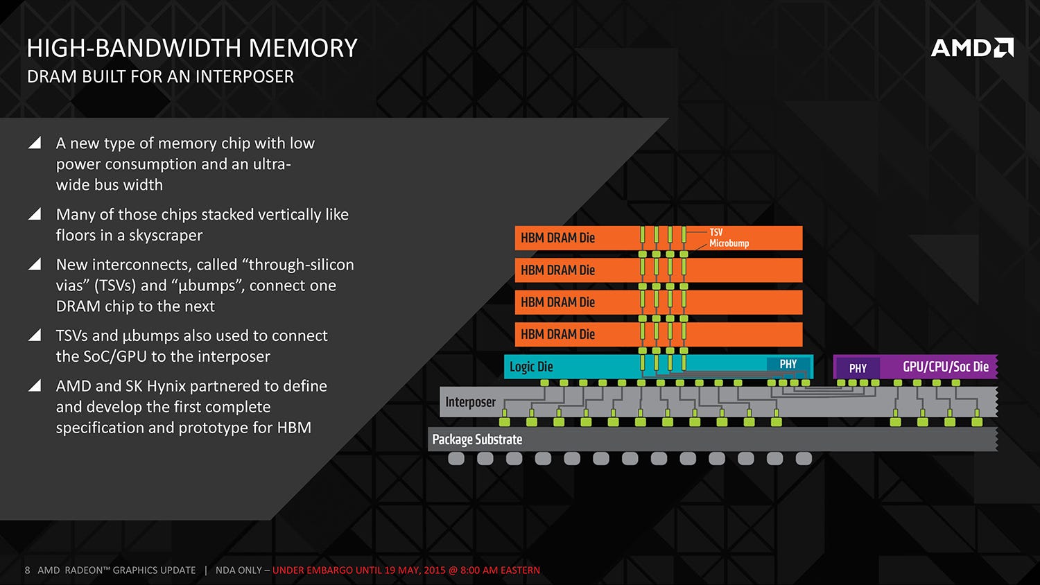
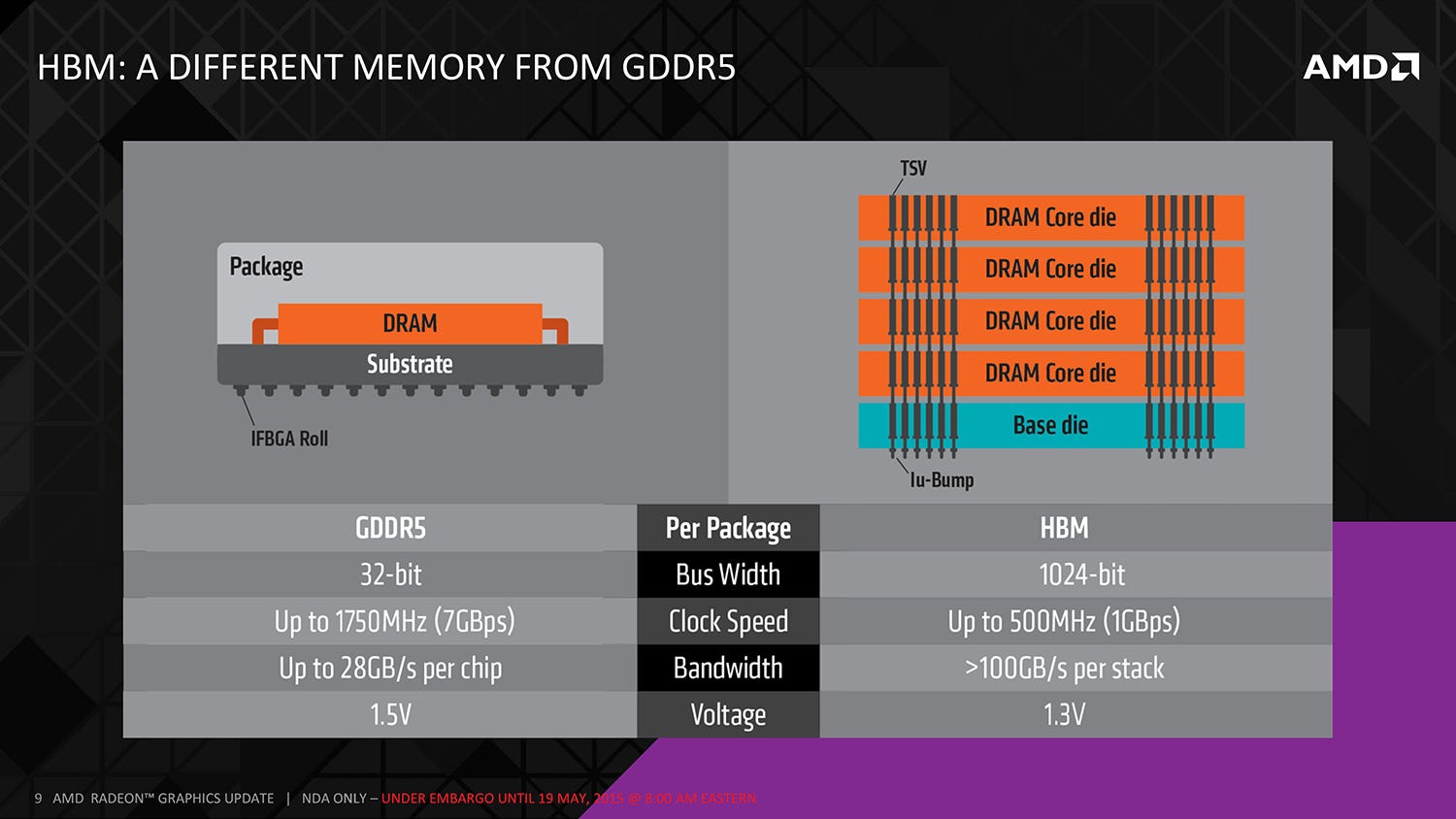
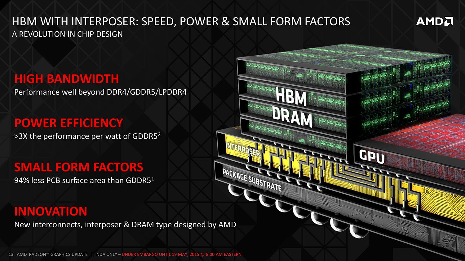
On a broader level, GPU performance is increasing at a rate that GDDR5 cannot match, potentially increasing the chance of memory bottlenecks. A new solution is required, and that's where HBM comes to the fore. As opposed to the GDDR5 system of individual modules soldered to the board and connected to the GPU's memory controller, HBM offers up a much more refined solution. Individual memory modules are stacked one on top of another, connected by 'through-silicon-vias' (TSVs) and separated by microbumps. A single GDDR5 chip on a 32-bit interface offers up 28GB/s of throughput. In contrast, an HBM stack is 1024 bits wide, with over 100GB/s of bandwidth (AMD partner Hynix has a more precise 128GB/s metric), achieved with a significant drop in voltage too. Efficiency is also increased by sitting both the GPU core and the HBM stacks on an 'interposer' which brings the two elements much closer together.
AMD revealed that each HBM stack has four 256MB memory chips sandwiched vertically, and that its initial products will have four of these stacks grouped around its new GPU (widely believed - but currently unconfirmed - to be a larger, more powerful iteration of its existing GCN tech). So in theory we are looking at a GPU with 512GB/s of total bandwidth (vs 320GB/s on R9 290X and 336.5GB/s on Nvidia's Titan X), but the slightly less welcome news is that memory capacity won't improve over AMD's existing flagships. Joe Macri played this down during the conference call, but in a world where modern games are hitting the 4GB threshold at 1440p, this is a concern, particularly as it's widely rumoured that Nvidia's forthcoming GTX 980 Ti ships with 6GB of GDDR5. On the flipside, the extra bandwidth could help with memory intensive applications where we currently see a bottleneck - multi-sampling anti-aliasing (MSAA) for example.
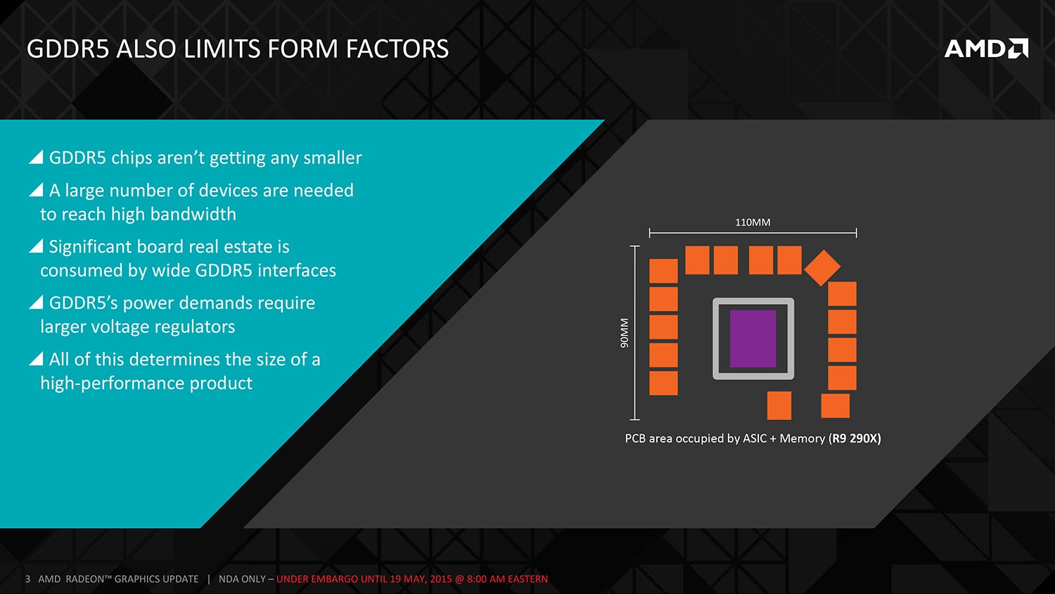
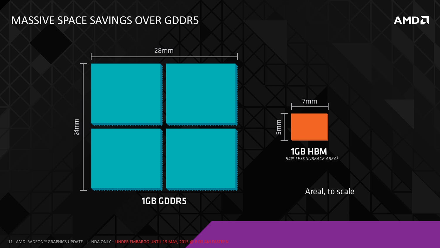
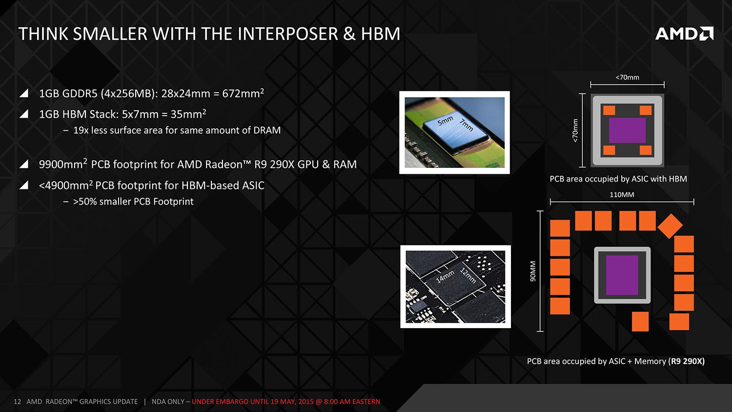
Consolidating memory modules into a much tighter space has other advantages too. The space taken in mounting individual modules to the PCB is one of the main reasons why graphics cards are so large. Typically, four 256MB chips occupy 672mm2 of area, while the HBM stacked equivalent is just 35mm2. Even factoring in the arrival of 512MB GDDR5 modules, the space saving is still immense. AMD says that the PCB footprint of its R9 290X GPU and RAM is 9900mm2, and says that an HBM-based equivalent would be less than 4900mm2. That's a PCB that's over 50 per cent smaller - so potentially, the upcoming Radeon flagship should not only be immensely powerful but there may well be small form-factor PC applications too.
Outside of the graphics card applications, we should expect to see HBM techniques applied to other technologies too. At the moment, AMD's APUs - which combine x86 CPU cores with GCN integrated graphics - are hamstrung by the low bandwidth of DDR3 memory. While adding HBM RAM will add to the cost, we could finally start to see APUs capable of enthusiast-level gaming. On top of that, some future version of HBM technology could find its way into a future console too. AMD's partner on the HBM project - memory specialist Hynix - has already revealed the roadmap for HBM, giving us some idea of future scalability. Those 1GB stacks will transform into 4GB or even 8GB stacks while bandwidth will double.
So the big question is, where does this leave AMD's arch-rival, Nvidia? In the short term, a potential Radeon R9 390X will go head-to-head with GTX 980 Ti, a slightly cut-down version of the Titan X. It should be a fascinating contest as Nvidia's product will probably have more memory, but it won't have the bandwidth advantages of HBM.
The question is to what extent higher memory throughput will have on game performance. Lavish amounts of bandwidth are great for aspects like post-process effects and MSAA, but the console designs practically demand that bandwidth-heavy compute is tucked into the GPU's L2 cache. On top of that, with current PC games, overclocking the GPU core is shown to have a much greater impact on frame-rates than overclocking GDDR5. It may well be that in the short term at least, the power efficiency and space-saving inherent in the HBM design are where we'll see the most noticeable differences.
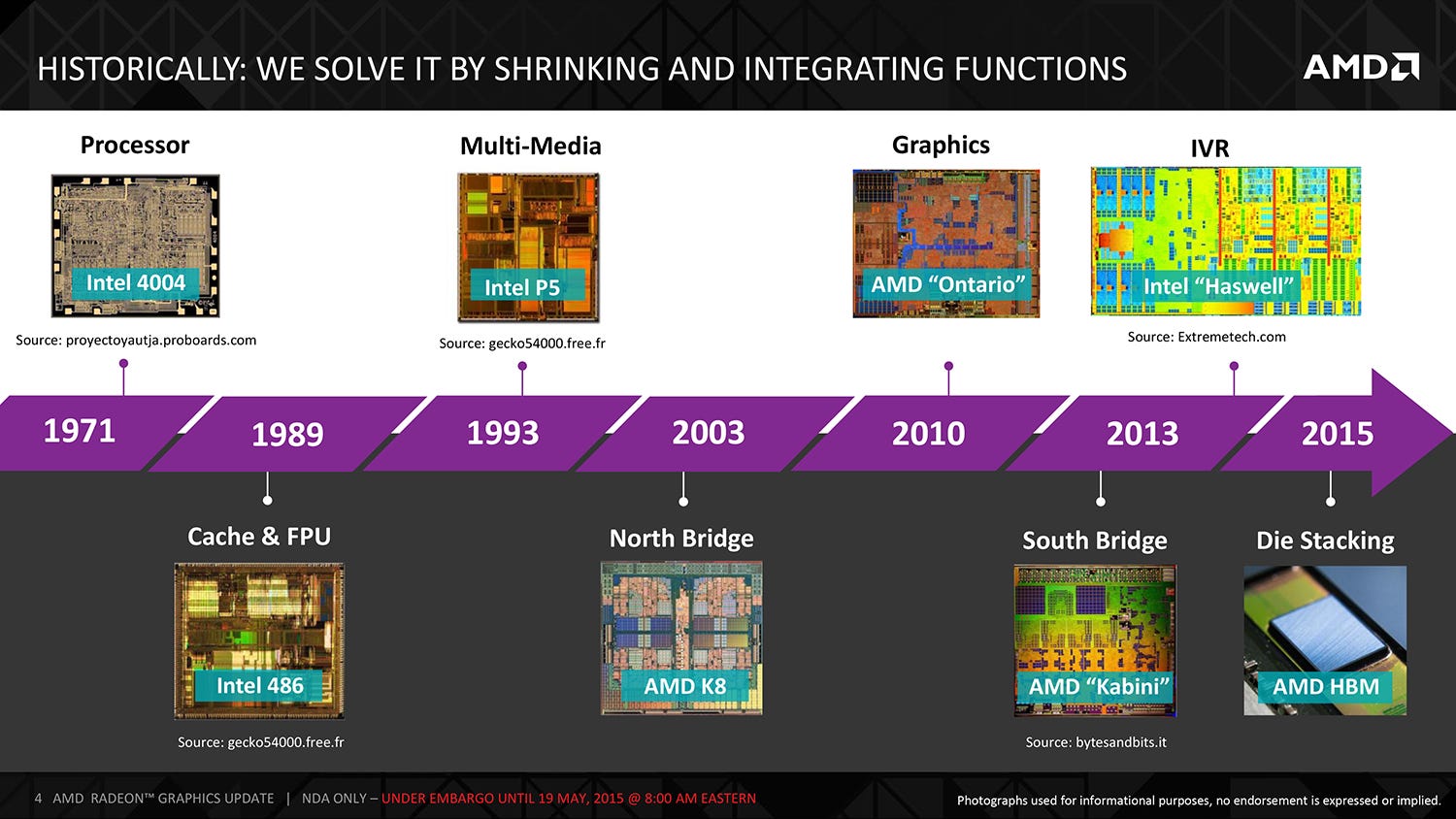
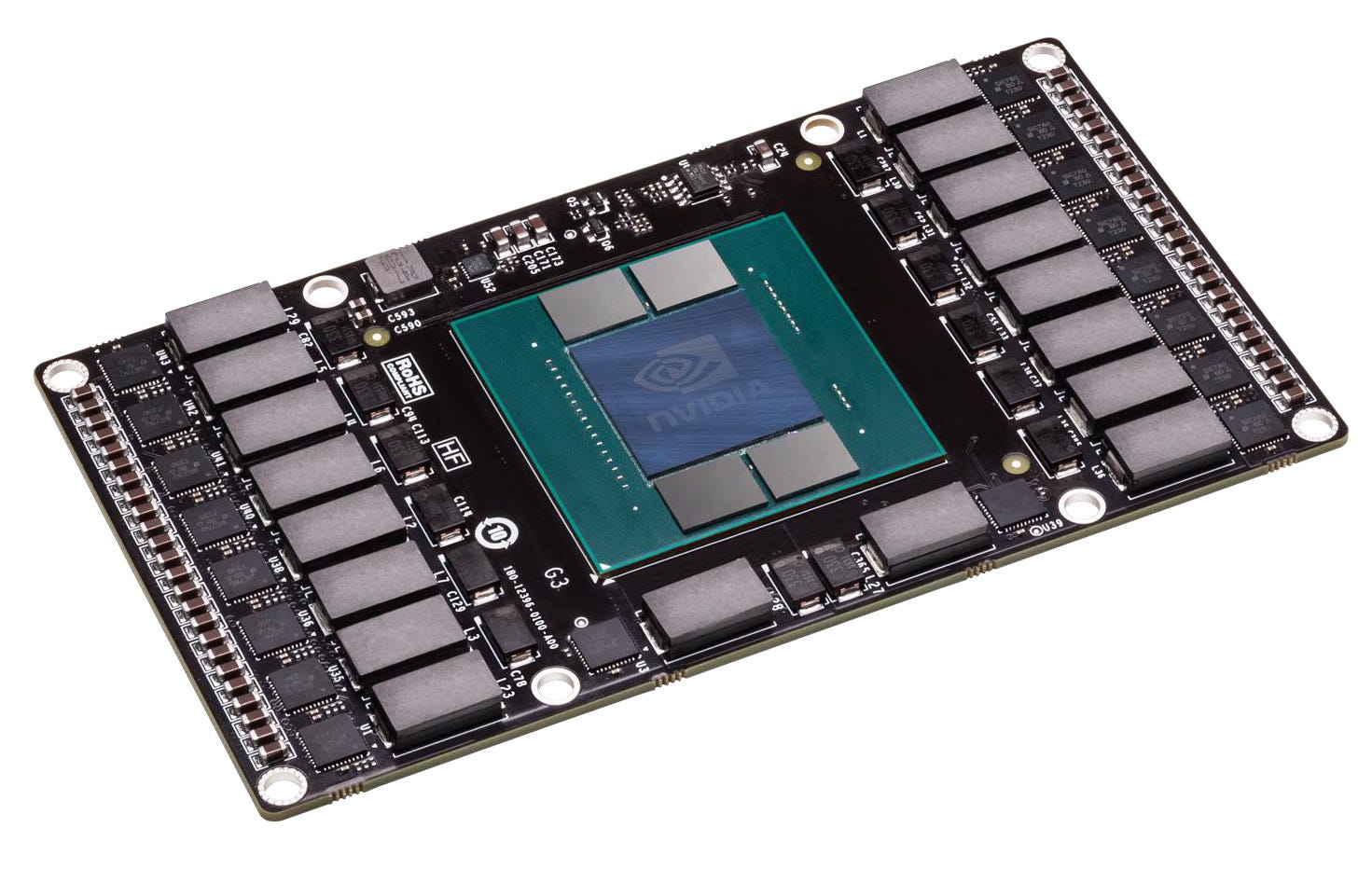
However, it's worth stressing that HBM is not a wholly proprietary technology. The concept of stacked memory modules is hardly unique thinking: AMD says it has been working on the tech for seven years, but the principles behind it are hardly a secret and Nvidia has already shown off a test vehicle showcasing its own version (pictured above). It's a part of its next-gen Pascal architecture that's due to arrive in 2016. But it's AMD that will be first to market with stacked memory and we can't wait to put it through its paces.